PCB copper cladding important tips
PCB copper cladding must pay attention to these, otherwise do not clad copper!
The so-called copper PCB , is the PCB on the unused space as a reference surface, and then filled with solid copper, these copper areas are also known as copper filling. The significance of copper cladding is to reduce the impedance of the ground, improve the ability to resist interference; reduce the voltage drop, improve the efficiency of the power supply; connected to the ground, you can also reduce the loop area. Also for the purpose of PCB welding as far as possible without deformation, most PCB manufacturers will also require PCB designers in the open areas of the PCB filled with copper or grid-like ground, copper cladding if not handled properly, it will not be worth the loss, whether copper cladding is “more good than bad” or ” more harm than good”?
We all know that in the case of high frequency, the printed circuit board wiring distributed capacitance will play a role, when the length is greater than the corresponding wavelength of noise frequency 1/20 when the antenna effect will be generated, the noise will be emitted outward through the wiring, if there is a bad ground in the PCB copper cladding words, copper cladding has become a tool for the spread of noise, therefore, in high-frequency PCB[1] , do not think that the ground line of a certain place connected Therefore, in high-frequency circuits, do not think that the ground wire is connected to the ground somewhere, which is the “ground wire”, but must be less than λ/20 spacing, punching holes in the wiring, and the ground plane of the multi-layer board “good ground”. If the copper cladding is handled properly, the copper cladding not only has increased current, but also plays a dual role in shielding interference.
Copper cladding generally has two basic ways, that is, large area of copper cladding and grid copper, often asked, large area of copper cladding or grid copper cladding is good, not good generalization. Why? Large area copper cladding, with increased current and shielding dual role, but large area copper cladding, if the wave soldering, the board may be warped, or even blistering. Therefore, large area copper, generally will also open a few slots to alleviate the copper foil blistering, simple grid copper cladding is mainly shielding role, the role of increasing the current is reduced, from the perspective of heat dissipation, the grid has the benefit (it reduces the copper heating surface) and play a certain role in electromagnetic shielding. However, it should be noted that the grid is made up of staggered direction of the line, we know that for the circuit, the width of the line for the board’s operating frequency is its corresponding “electrical length” (the actual size divided by the operating frequency corresponding to the digital frequency can be obtained, see the relevant books), when the operating frequency is not very high When the operating frequency is not very high, perhaps the role of the grid line is not very obvious, once the electrical length and the working frequency match, it is very bad, you will find that the circuit simply can not work properly, everywhere in the emission of signals that interfere with the work of the system. So for colleagues who use the grid, my advice is to choose according to the design of the board work, do not hold on to one thing not to put. Therefore, high-frequency pcb circuits with high requirements for anti-interference more grid, low-frequency PCB circuits with high current circuits, such as the common use of complete copper laying.Fubon Precision Electronics is a one-stop High-quality electronic manufacturing and solution service provider that integrates PCB and PCBA manufacturing[1] , electronic component procurement, SMT and assembly testing, and supply chain construction, Contact Fubon Precision[2] if you haven’t finished your PCB design so that our PCBA solution[3] specialists can offer helpful advice and solutions.

Having said that, then we are in the copper cladding, in order to make the copper cladding to achieve our desired results, then the copper cladding needs to pay attention to what issues:
2, the single point of connection to different ground, the practice is connected by 0 ohm resistors[1] or magnetic beads or inductors.
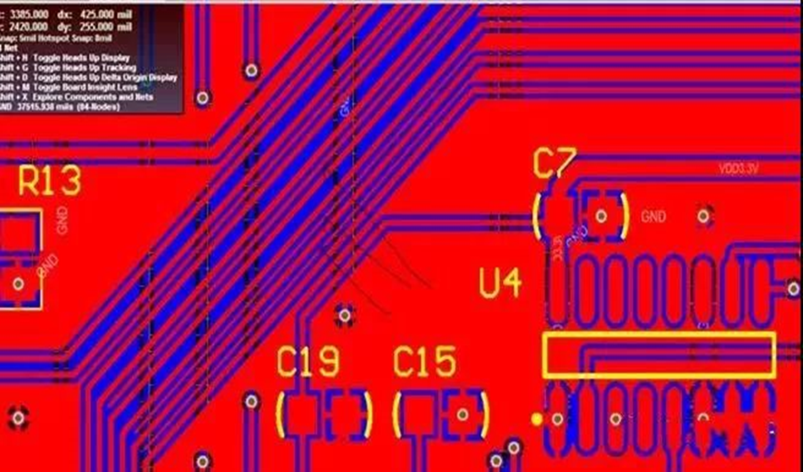
3, copper cladding near the crystal oscillator, the crystal in the circuit for a high-frequency emission source, the practice is to copper cladding around the crystal, and then the crystal’s shell is grounded separately.
4, the PCB island (dead zone) problem, if you feel large, then define a ground over the hole to add in it does not cost much.
5, in the beginning of the wiring, the ground should be treated equally, when the line should be the ground line, can not rely on the copper cladding by adding a hole to eliminate the ground pins for the connection, which is not good.
6, in the board as far as possible do not have a sharp angle (“= 180 degrees), because from the electromagnetic point of view, this constitutes a transmitting antenna! For the other will always have an impact only is large or small, I recommend the use of rounded edges line.
7, the middle layer of the multi-layer pcb[1] board wiring open area, do not cover copper. Because you are more difficult to make this copper cladding “good ground”.
8, the equipment inside the metal, such as metal heat sink, metal reinforcement, etc., must be achieved “good grounding.
9, the three-terminal voltage regulator heat dissipation metal block, must be well grounded. Crystal near the grounding isolation tape, must be well grounded. In short: PCB copper cladding, if the grounding problem is handled well, is certainly “more good than bad”, it can reduce the signal line reflow area, reduce the signal external electromagnetic interference.
Keywords: copper PCB[1] , multi-layer pcb[2] , resistors[3] , PCBA manufacturing[4] ,, PCBA solution[5] ,, Fubon Precision[6]