Description
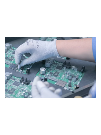
Electronic circuits are created using the through-hole assembly technique, in which the elements are inserted using leads. It describes the installation procedure in which the leads are inserted into the pre-drilled holes and the components are soldered to the board using either wave solder or manual soldering.
PCB design evolved from single-sided to double-sided, and finally to multi-layer boards. It is challenging to adapt through-hole assembly to the needs of contemporary electronics PCB. In today’s PCB manufacturing, SMT Technology has essentially taken the place of through-hole construction. It is important to keep in mind that through-hole assembly is not very effective for multi-layer PCBs because it consumes board area on every layer.
Features of the through-hole PCB assembly
- High reliability
- Easy to operate manually
- Higher durability
- Lower manufacturing efficiency
- Limited PCB design
Applications of Through-hole PCB Assembly
Through-hole components (THCs) are appropriate for high-reliability items that require a metallurgical bonding between layers. Since their leads pass via board perforations, they can resist greater environmental stress. Because of this, through-hole PCB assembly is frequently used in aerospace and military items that could be damaged by high temperatures, collisions, or rapid acceleration. Through-hole technology is also utilized in testing and prototypes, which may necessitate human replacement and correction.
Advantages And Disadvantages Of Through-Hole Assembly
For items that are prepared to be subjected to mechanical stress, through-hole mounting suggests a greater mechanical connection. Additionally, through-hole assembly is popular for testing and prototyping and is simple to replace and tune manually. Because through-hole component leads must pass through time-consuming and expensive holes on the board. Multi-layer PCBs routing space is also constrained by through-hole mounting because all layers of the boards must be covered by the drilled holes. Through-hole mounting soldering relies on wave soldering or hand soldering, which presents challenges for reliability and repeatability as well as decreased manufacturing efficiency.

