

")
")
")
Description
Basically speaking, HDI PCB means high density interconnect PCB. These boards feature high wiring density for each unit surface area. Microvia PCB serves as interconnectors between the HDI layers and PCBs.
When making use of these PCBs, you’ll discover that they feature fine spaces and lines, minor vias, high connector pad density and capture pads. They facilitate electrical performance, coupled with reducing their application’s weight and size.
These boards’ effectiveness serves as another option to using the expensive high-layer laminated boards. These boards have great characteristics such as high electrical frequency and speed, and they are lightweight. This is why they are useful for different applications.
Advantages of HDI PCBs
HDI PCBs come with many advantages. This is what makes HDI PCB manufacturers love to use them. Let’s quickly take a look at them:
1 Reduction in heat transfer
One advantage of having HDI PCB is that there is a reduced transfer of heat. One reason for this is that heat travels short distances before finding a way to escape the HDI PCB. It also comes with a great design, which helps it undergo high thermal expansion. This in turn increases the PCB’s lifespan.
2 Manages thermal conductivity
The presence of vias assists the High density PCB in the transmission of current between the components. This vial can be filled either with non-conductive or conductive materials.
The HDI PCB’s functionality can be improved by placing the via-in-pad and blind vias components together. By reducing the transmission distance between these components, the transmission times and crossing delays are reduced. With these, your HDI PCB will have a strong signal.
3 Smaller form factors
Regarding saving space, HDI PCB is best. While giving your HDI PCB a design, you can reduce the number of layers. With this, you’ll have a smaller PCB having vias that reduces performance and looks visible to an individual
4 Less power usage
One advantage of having HDI PCBs is its ability to use less battery power. This is possible as a result of the technology utilized during the manufacturing.
This type of technology entails keeping its electrical components, which reduces energy loss. This leads to an extension of your battery lifespan. Using vias rather than through holes makes the High density PCB great at lessening power usage.
Incorporating components
Since the PCB’s space can be minimized for the components, it is possible to integrate whatever details you desire on the board. Also, depending on your PCB’s design, you can increase or decrease the number of layers. Another way of integrating these digikey.com is populating the two sides of the boards. Also, this depends on your HDI PCB’s application and design.
Different designs
With HDI PCBs, your application can have different designs. They come in different types as well. For example, you may have rigid, flexible pcb, or a mix of both for your application.
HDI PCB: Types
HDI PCB comes in different types. Although they are different, with respect to designs, they have the same function. The type you decide to choose depends on the application you are using. Let’s quickly consider the types.
1 Flex HDI PCB
Flex HDI PCB is composed of flexible plastic. This material permits the board to form different shapes. This offers lots of benefits when compared with rigid boards.
The board’s flexibility also allows you to move or bend easily during the process of application without bringing damage to the circuits that are present on the board. One disadvantage with this board type is that designing and manufacturing it costs a lot. However, they come with numerous benefits.
The heavy wiring found in advanced equipment like satellites can be replaced with these PCBs. They are lighter and make use of little space, making them great for such use. Another benefit is that it features different designs like multilayer, single-sided, or double-sided designs.
2 Rigid HDI PCB
Asides the number of layers and sides that this HDI PCB has, it also comes in different rigidities. They are made up of a solid and rigid substrate material such as fiberglass. This kind of material prevents the bending of the HDI board. The application of this HDI PCB can be found on towers of most desktops.
3 Rigid-Flex HDI PCB
This is made up of a rigid circuit board, which attaches to a flexible board. The design’s complexity depends on whatever application you are using.
4 Multilayer HDI PCB
These boards have substrate boards of multiple layers with an insulating material that separates these layers. Just like HDI PCBs with double sides, either vias or through holes can be used in connecting the board’s electric circuits. Multilayer HDI PCBs are very beneficial because they use less space. Standard applications using this HDI board type include medical machinery, servers, handheld devices, and computers.
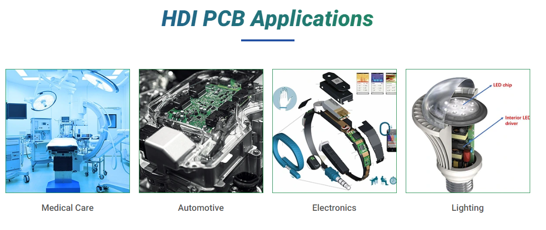
HDI PCB Application
Now, you may be thinking where HDI PCBs can be applied. These PCBs can be applied in many applications. Below are some of the applications where HDIN PCBs can be used:
1 Consumer Electronics
Consumer electronics has to do with those basic devices you find with most people. These include smartphones, computers, home appliances, laptops, entertainment systems, and recording devices.
The nature of these gadgets may require the use of lighter PCBs. HDI PCBs meet all these qualities, this is why HDI PCB manufacturers usually use them in producing these gadgets. However, there’s a need for manufacturers to work with the regulations already in place.
2 Medical Equipment
Regarding our health, electronics play a very significant role. The PCBs in the medical industry are highly specialized. This is to ensure they adhere strictly to the standards.
Some of these standards include having these HDI PCBs in small sizes and incorporating all the useful details. Another thing to consider here is that they have to adhere strictly to health standards. This is necessary to ensure the patients’ safety. Some medical devices prove the importance of HDI PCB. Some of them include scientific instruments, control systems, heart peacemakers, scanners, and monitors.
3 Industrial Applications
When dealing with highly-powered industrial apps, HDI PCBs are usually seen as the standard. This is because they consume less energy coupled with generating maximum output.
Asides from this, they have the ability to withstand harsh environments while they carry out their functions. Majority of HDI PCBs integrate thick copper on their boards. This ensures high current applications and its battery charges faster. These PCBs can be found in different industrial applications like electric bells, which measures the equipment used in measuring temperature and speed. Asides from this, they can be found in power equipment like generators and solar power panels.
4 Automotive Applications
Most automotives rely greatly on their electronic parts to run effectively. The application of HDI PCBs as well as other technologies can be done to sensor applications usually found in automotives.
Some other technologies like radar technology are also coming into the automotive industry. These technologies all function using HDI PCBs. The most common of these applications are engine management systems and car control systems. You can also find them in navigation devices, surrounding motors, and video and audio devices.
5 Aerospace Applications
The precision and durability offered by HDI ensures that they are great for the majority of aerospace applications. The turbulent and harsh environments that jets and airplanes go through need equipment that will withstand such stress.
To solve this problem, the majority of airplanes make use of HDI PCBs that are flexible. They usually have a small size and are lightweight. Asides from this, they also resist vibration effects. There are certain standards these HDI must meet in order to be utilized in the aerospace niche. This is because the airplanes’ safety relies on them.
Some of the well-known applications of HDI PCB are monitoring equipment like pressure cookers and accelerometer. You can also find them in equipment for testing.
6 Lighting Applications
The HDI PCB is also very useful in different LED applications. These LEDs are now becoming more popular as a result of technology change.
These lights are very beneficial because they are very efficient and only use up less power. HDI PCBs are usually found at the LED’s core. These components are close; this means that there is a reduced loss of energy to the surrounding. This ensures maximum output.
Conclusion
We hope we were able to answer all your questions regarding HDI PCBs. When choosing an HDI PCB, please make sure you check the specifications. These specifications include materials used and your HDI PCB design.
Additional information
| PCB Item | Manufacture Capacity |
|---|---|
| Layer Counts | 1–64L |
| Base Material | FR4,High-TGFR4 |
| Material Thickness(mm) | 0.40,0.60,0.80,1.00,1.20,1.50,1.60,2.0,2.4,3.2 4.0 5.0 6.0 |
| Max board size(mm) | 1200x400mm |
| Board Outline Tolerance | ±0.15mm |
| Board Thickness | 0.4mm-6.0mm |
| Thickness Tolerance | ±8% |
| Minimum line/space | 0.1mm |
| Min Annular Ring | 0.1mm |
| SMD Pitch | 0.3mm |
| Min Hole Size(mechanical) | 0.2mm |
| Min Hole Size(laser hole) | 0.1mm |
| Hole Size Tol(+/-) | PTH:±0.075mm;NPTH:±0.05mm |
| Hole Position Tol | ±0.075mm |
| HASL/LF HAL | 2.5um |
| Immersion Gold | Nickel 3-7um Au:1-5u" |
| Surface Finish | HAL,ENIG,Plated Gold,Immersion Gold,OSP |
| Copper Weight | 0.5–602 |
| Solder mask | Green, Blue,Black,White, Yellow, Red, Matt Green, Matt Black, Matt Blue |
| Slk screen | White, Black, Blue,Yellow |
| Acceptable File Format | Gerber fle,Powerpcb,CAD,AUTOCAD,ORCAD,P-CAD,CAM-350,CAM2000 |
| Certificate | ROSH,ISO9001 |