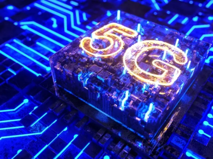
What are the Telecom PCB design considerations? – Printed circuit boards,consumer electronics,Telecom,Component,PCB manufacturing,mechanical
Printed circuit boards play a critical role in our advanced age of information technology, and telecommunications has become nearly synonymous with the PCBs that power them.
The world has come a long way since the age of telephone operators where people would line rows of desks connecting one call to another. Today, the Bureau of Labor Statistics estimates that just 5,000 workers in the United States are still classified as telephone operators, with many of these jobs expected to disappear in the coming decades.
The functionality of massive switchboards has followed the trend of virtually all consumer electronics: miniaturization. Calls and communications can now be placed across the world with little delay thanks to cell towers, satellites, and servers latticing the globe. Yet the speed at which we can communicate takes a tremendous amount of processing power – thus, the PCBs that power telecommunications must be reliable, durable, and above all else, functional.
Telecom PCB (Printed Circuit Board) design considerations are crucial for ensuring the reliable and efficient operation of telecommunications equipment and devices. These considerations encompass various aspects of the PCB design process, from the layout of components to signal integrity and thermal management. Here are some key considerations:
Signal Integrity: a. Controlled Impedance: Maintain consistent impedance throughout the transmission lines to minimize signal reflection and loss. b. Crosstalk Mitigation: Keep signal traces adequately spaced and use ground planes and shielding to reduce electromagnetic interference (EMI) and crosstalk. c. Signal Routing: Use differential pairs for high-speed data signals, and follow best practices for minimizing signal path length and avoiding sharp corners.
Power Distribution: a. Power Planes: Design proper power and ground planes to provide a stable power distribution network and reduce noise. b. Decoupling Capacitors: Place decoupling capacitors strategically near high-power components to suppress voltage fluctuations and improve signal quality.
Component Placement: a. Thermal Considerations: Position heat-generating components strategically for efficient heat dissipation and consider adding thermal vias. b. High-Speed Components: Place high-speed components closer to each other and minimize trace lengths to reduce signal delay. c. Mechanical Fit: Ensure that components fit within the enclosure and that connectors align correctly.
EMI/EMC Compliance: a. Shielding: Use shielding techniques, such as grounded enclosures and conductive gaskets, to contain electromagnetic emissions. b. Filtering: Incorporate EMI filters to suppress conducted and radiated emissions. c. Grounding: Implement a solid ground plane and ensure proper grounding practices to minimize EMI and ensure EMC compliance.
Environmental Considerations: a. Temperature Range: Choose PCB materials and components suitable for the operating temperature range of the telecom equipment. b. Environmental Protection: Consider conformal coating or encapsulation to protect against moisture, dust, and contaminants.
Design for Manufacturability (DFM) and Design for Test (DFT): a. Minimize Complexity: Simplify the design to reduce manufacturing and testing challenges. b. Test Points: Include test points for easy troubleshooting and testing during production and maintenance.
Reliability: a. Redundancy: Incorporate redundancy where necessary for fault tolerance and reliability. b. Component Selection: Choose high-quality components from reputable suppliers. c. Thermal Management: Implement proper heat sinks, fans, or other cooling solutions to prevent overheating.
PCB Stackup: a. Layer Stackup: Select an appropriate layer count and stackup configuration to meet signal integrity and EMI requirements.
Compliance with Standards: a. Ensure that the PCB design complies with relevant industry standards and regulations, such as IPC standards for PCB manufacturing.
Documentation: a. Create comprehensive design documentation, including schematics, layout files, and BOM (Bill of Materials), for manufacturing and troubleshooting.
Effective telecom PCB design requires a multidisciplinary approach that takes into account electrical, mechanical, thermal, and environmental factors. Collaboration between PCB designers, electrical engineers, and mechanical engineers is often necessary to achieve the desired performance and reliability in telecommunications equipment.
At Fubon Precision, we have over 13 years of industry experience. Importantly, we have dealt with a wide range of telecom providers. We are therefore well-poised to understand the various issues than plague the industry and how robust testing can help overcome these issues. To know more, please explore our PCB manufacturing services for Telecommunication Industry!