Innovation and Integration in PCB Design
Innovation and integration are crucial aspects of modern PCB (Printed Circuit Board) design, driving advancements in electronics technology. Here are some key points related to innovation and integration in PCB design:
Miniaturization and Component Density:
Innovative Packaging Techniques: Smaller form factors and increased component density are achieved through innovative packaging techniques like System-in-Package (SiP) and Chip-on-Board (CoB).
Advanced Materials: The use of advanced materials with higher thermal conductivity and reduced signal loss facilitates the miniaturization of PCBs.
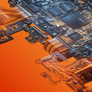
Multi-layer PCBs:
Increased Integration: Multi-layer PCBs allow for higher integration by accommodating more components and complex routing in a smaller space.
Innovative Stack-up Designs: Optimized stack-up designs help in managing signal integrity, power distribution, and thermal considerations.
High-Frequency Design:
Innovative Signal Integrity Techniques: High-frequency designs require innovative signal integrity techniques, such as controlled impedance traces, to minimize signal degradation and ensure reliable performance.
Integration of RF Components: Integration of radio frequency (RF) components directly onto the PCB enables the design of compact and efficient wireless communication devices.
Flexible and Rigid-Flex PCBs:
Innovative Flex Circuit Designs: Flexible and rigid-flex PCBs offer new design possibilities for applications with space constraints or dynamic form factors.
Integration of Sensors and Actuators: Flexibility allows for the integration of sensors and actuators in wearable devices and other applications.
Advanced Manufacturing Techniques:
Innovative PCB Manufacturing Processes: Advancements in manufacturing processes, such as additive manufacturing and 3D printing, contribute to innovative PCB designs.
Integrated Manufacturing and Assembly: Integrating PCB design with the manufacturing and assembly processes enhances efficiency and reduces time-to-market.
Power Management:
Innovative Power Distribution Networks: Efficient power management is critical. Innovative power distribution networks, including advanced voltage regulation and energy harvesting techniques, contribute to better energy efficiency.
Integration of Power Electronics: Integrating power electronics on the PCB itself can reduce the need for external power modules.
Smart and IoT Integration:
Integration of Sensors and Microcontrollers: PCBs play a key role in the integration of sensors and microcontrollers in IoT devices.
Innovative IoT Connectivity Solutions: Incorporating innovative connectivity solutions for IoT, such as low-power wireless communication protocols, enables seamless integration into the Internet of Things ecosystem.
Environmental Considerations:
Innovative Materials for Sustainability: There’s an increasing focus on using environmentally friendly materials and manufacturing processes in PCB design.
Integration of Energy-Efficient Components: Designing with energy-efficient components contributes to overall sustainability.
In summary, innovation in PCB design involves incorporating new technologies and methodologies to improve performance, reduce size, and enhance functionality. Integration is about bringing together diverse components and technologies on a single board to create efficient, compact, and high-performance electronic systems. Both aspects are essential for staying at the forefront of electronic design in a rapidly evolving technological landscape.